- 您现在的位置:买卖IC网 > Sheet目录3881 > PIC18F8720T-E/PT (Microchip Technology)IC PIC MCU FLASH 64KX16 80TQFP
2004 Microchip Technology Inc.
DS39609B-page 103
PIC18F6520/8520/6620/8620/6720/8720
10.0
I/O PORTS
Depending on the device selected, there are either
seven or nine I/O ports available on PIC18FXX20
devices. Some of their pins are multiplexed with one or
more alternate functions from the other peripheral fea-
tures on the device. In general, when a peripheral is
enabled, that pin may not be used as a general
purpose I/O pin.
Each port has three registers for its operation. These
registers are:
TRIS register (data direction register)
PORT register (reads the levels on the pins of the
device)
LAT register (output latch)
The Data Latch (LAT register) is useful for read-modify-
write operations on the value that the I/O pins are
driving.
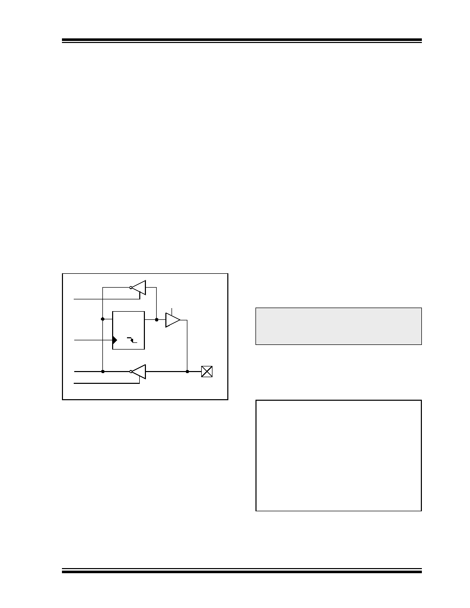
A simplified version of a generic I/O port and its
operation is shown in Figure 10-1.
FIGURE 10-1:
SIMPLIFIED BLOCK
DIAGRAM OF PORT/LAT/
TRIS OPERATION
10.1
PORTA, TRISA and LATA
Registers
PORTA is a 7-bit wide, bidirectional port. The corre-
sponding data direction register is TRISA. Setting a
TRISA bit (= 1) will make the corresponding PORTA pin
an input (i.e., put the corresponding output driver in a
high-impedance mode). Clearing a TRISA bit (= 0) will
make the corresponding PORTA pin an output (i.e., put
the contents of the output latch on the selected pin).
Reading the PORTA register reads the status of the
pins, whereas writing to it will write to the port latch.
The Data Latch register (LATA) is also memory
mapped. Read-modify-write operations on the LATA
register, read and write the latched output value for
PORTA.
The RA4 pin is multiplexed with the Timer0 module
clock input to become the RA4/T0CKI pin. The RA4/
T0CKI pin is a Schmitt Trigger input and an open-drain
output. All other RA port pins have TTL input levels and
full CMOS output drivers.
The RA6 pin is only enabled as a general I/O pin in
ECIO and RCIO Oscillator modes.
The other PORTA pins are multiplexed with analog
inputs and the analog VREF+ and VREF- inputs. The
operation of each pin is selected by clearing/setting the
control bits in the ADCON1 register (A/D Control
Register 1).
The TRISA register controls the direction of the RA
pins, even when they are being used as analog inputs.
The user must ensure the bits in the TRISA register are
maintained set when using them as analog inputs.
EXAMPLE 10-1:
INITIALIZING PORTA
Q
D
CK
WR LAT +
Data Latch
I/O pin
RD Port
WR Port
TRIS
RD LAT
Data Bus
Note:
On a Power-on Reset, RA5 and RA3:RA0
are configured as analog inputs and read
as ‘0’. RA6 and RA4 are configured as
digital inputs.
CLRF
PORTA
; Initialize PORTA by
; clearing output
; data latches
CLRF
LATA
; Alternate method
; to clear output
; data latches
MOVLW
0x0F
; Configure A/D
MOVWF
ADCON1
; for digital inputs
MOVLW
0xCF
; Value used to
; initialize data
; direction
MOVWF
TRISA
; Set RA<3:0> as inputs
; RA<5:4> as outputs
发布紧急采购,3分钟左右您将得到回复。
相关PDF资料
PIC18F4439T-E/ML
IC PIC MCU FLASH 6KX16 44QFN
XF2J-2824-11
CONN FPC 28POS 0.5MM SMT
PIC18F4439T-E/PT
IC PIC MCU FLASH 6KX16 44TQFP
PIC18F6585T-I/PT
IC PIC MCU FLASH 24KX16 64TQFP
PIC18LF8525T-I/PT
IC PIC MCU FLASH 24KX16 80TQFP
PIC18F6720T-E/PT
IC PIC MCU FLASH 64KX16 64TQFP
PIC18F4539T-E/PT
IC PIC MCU FLASH 12KX16 44TQFP
PIC16F685-I/P
IC PIC MCU FLASH 4KX14 20DIP
相关代理商/技术参数
PIC18F8720T-I/PT
功能描述:8位微控制器 -MCU 128KB 3840 RAM 68I/O RoHS:否 制造商:Silicon Labs 核心:8051 处理器系列:C8051F39x 数据总线宽度:8 bit 最大时钟频率:50 MHz 程序存储器大小:16 KB 数据 RAM 大小:1 KB 片上 ADC:Yes 工作电源电压:1.8 V to 3.6 V 工作温度范围:- 40 C to + 105 C 封装 / 箱体:QFN-20 安装风格:SMD/SMT
PIC18F8721-I/PT
功能描述:8位微控制器 -MCU 128kBF 4096RM 40MHz nonoWatt RoHS:否 制造商:Silicon Labs 核心:8051 处理器系列:C8051F39x 数据总线宽度:8 bit 最大时钟频率:50 MHz 程序存储器大小:16 KB 数据 RAM 大小:1 KB 片上 ADC:Yes 工作电源电压:1.8 V to 3.6 V 工作温度范围:- 40 C to + 105 C 封装 / 箱体:QFN-20 安装风格:SMD/SMT
PIC18F8721T-I/PT
功能描述:8位微控制器 -MCU 128kBF 4096RM 40MHz nonoWatt RoHS:否 制造商:Silicon Labs 核心:8051 处理器系列:C8051F39x 数据总线宽度:8 bit 最大时钟频率:50 MHz 程序存储器大小:16 KB 数据 RAM 大小:1 KB 片上 ADC:Yes 工作电源电压:1.8 V to 3.6 V 工作温度范围:- 40 C to + 105 C 封装 / 箱体:QFN-20 安装风格:SMD/SMT
PIC18F8722 DEVELOPMENT BOARD KIT
功能描述:DEVELOPMENT BOARD FOR PIC18F8722 RoHS:否 类别:编程器,开发系统 >> 通用嵌入式开发板和套件(MCU、DSP、FPGA、CPLD等) 系列:- 标准包装:1 系列:PICDEM™ 类型:MCU 适用于相关产品:PIC10F206,PIC16F690,PIC16F819 所含物品:板,线缆,元件,CD,PICkit 编程器 产品目录页面:659 (CN2011-ZH PDF)
PIC18F8722 DEVELOPMENT KIT
功能描述:EMBEDDED C DEVELOPMENT KIT RoHS:否 类别:编程器,开发系统 >> 通用嵌入式开发板和套件(MCU、DSP、FPGA、CPLD等) 系列:PIC® 产品培训模块:Blackfin® Processor Core Architecture Overview
Blackfin® Device Drivers
Blackfin® Optimizations for Performance and Power Consumption
Blackfin® System Services 特色产品:Blackfin? BF50x Series Processors 标准包装:1 系列:Blackfin® 类型:DSP 适用于相关产品:ADSP-BF548 所含物品:板,软件,4x4 键盘,光学拨轮,QVGA 触摸屏 LCD 和 40G 硬盘 配用:ADZS-BFBLUET-EZEXT-ND - EZ-EXTENDER DAUGHTERBOARDADZS-BFLLCD-EZEXT-ND - BOARD EXT LANDSCAP LCD INTERFACE 相关产品:ADSP-BF542BBCZ-4A-ND - IC DSP 16BIT 400MHZ 400CSBGAADSP-BF544MBBCZ-5M-ND - IC DSP 16BIT 533MHZ MDDR 400CBGAADSP-BF542MBBCZ-5M-ND - IC DSP 16BIT 533MHZ MDDR 400CBGAADSP-BF542KBCZ-6A-ND - IC DSP 16BIT 600MHZ 400CSBGAADSP-BF547MBBCZ-5M-ND - IC DSP 16BIT 533MHZ MDDR 400CBGAADSP-BF548BBCZ-5A-ND - IC DSP 16BIT 533MHZ 400CSBGAADSP-BF547BBCZ-5A-ND - IC DSP 16BIT 533MHZ 400CSBGAADSP-BF544BBCZ-5A-ND - IC DSP 16BIT 533MHZ 400CSBGAADSP-BF542BBCZ-5A-ND - IC DSP 16BIT 533MHZ 400CSBGA
PIC18F8722-E/PT
功能描述:8位微控制器 -MCU 128 KB FL 3936 RAM 25 MHz RoHS:否 制造商:Silicon Labs 核心:8051 处理器系列:C8051F39x 数据总线宽度:8 bit 最大时钟频率:50 MHz 程序存储器大小:16 KB 数据 RAM 大小:1 KB 片上 ADC:Yes 工作电源电压:1.8 V to 3.6 V 工作温度范围:- 40 C to + 105 C 封装 / 箱体:QFN-20 安装风格:SMD/SMT
PIC18F8722-I/PT
功能描述:8位微控制器 -MCU 128 KB FL 4K RAM 70 I/O RoHS:否 制造商:Silicon Labs 核心:8051 处理器系列:C8051F39x 数据总线宽度:8 bit 最大时钟频率:50 MHz 程序存储器大小:16 KB 数据 RAM 大小:1 KB 片上 ADC:Yes 工作电源电压:1.8 V to 3.6 V 工作温度范围:- 40 C to + 105 C 封装 / 箱体:QFN-20 安装风格:SMD/SMT
PIC18F8722T-E/PT
功能描述:8位微控制器 -MCU 128 KB FL 3936 RAM 25MHz RoHS:否 制造商:Silicon Labs 核心:8051 处理器系列:C8051F39x 数据总线宽度:8 bit 最大时钟频率:50 MHz 程序存储器大小:16 KB 数据 RAM 大小:1 KB 片上 ADC:Yes 工作电源电压:1.8 V to 3.6 V 工作温度范围:- 40 C to + 105 C 封装 / 箱体:QFN-20 安装风格:SMD/SMT